
Practical tests of neutron transmission imaging with a superconducting kinetic-inductance sensor
Published:
Abstract
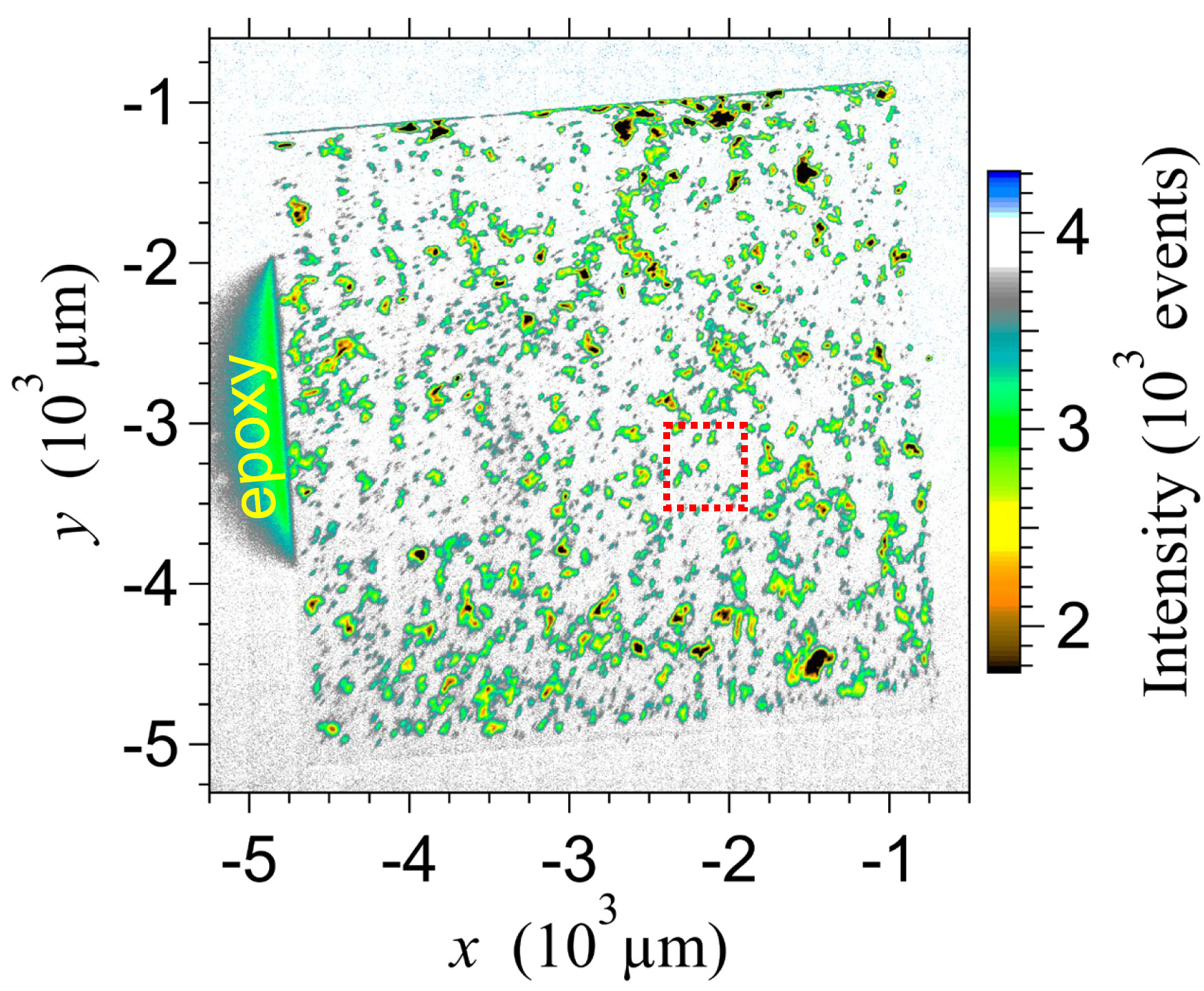
Samples were examined using a superconducting (Nb) neutron imaging system employing a delay-line technique which in previous studies was shown to have high spatial resolution. We found excellent correspondence between neutron transmission and scanning electron microscope (SEM) images of Gd islands with sizes between 15 and 130 micrometer which were thermally-sprayed onto a Si substrate. Neutron transmission images could be used to identify tiny voids in a thermally-sprayed continuous Gd2O3 film on a Si substrate which could not be seen in SEM images. We also found that neutron transmission images revealed pattern formations, mosaic features and co-existing dendritic phases in Wood’s metal samples with constituent elements Bi, Pb, Sn and Cd. These results demonstrate the merits of the current-biased kinetic inductance detector (CB-KID) system for practical studies in materials science. Moreover, we found that operating the detector at a more optimal temperature (7.9 K) appreciably improved the effective detection efficiency when compared to previous studies conducted at 4 K. This is because the effective size of hot-spots in the superconducting meanderline planes increases with temperature, which makes particle detections more likely.
T. D. Vu, H. Shishido, K. Aizawa, K. M. Kojima, T. Koyama, K. Oikawa, M. Harada, T. Oku, K. Soyama, S. Miyajima, M. Hidaka, S. Y. Suzuki, M. M. Tanaka, A. Malins, M. Machida, S. Kawamata & T. Ishida
Nuclear Instruments and Methods in Physics Research Section A: Accelerators, Spectrometers, Detectors and Associated Equipment 1006, 165411 (2021)
DOI: 10.1016/j.nima.2021.165411
PDF: download
ArXiv: https://arxiv.org/abs/2105.03612